


… by Vamsi Krishna Yaddanapudi, Technical Director (Electronics), Synopsys India
The demand for higher data rates is no longer just a trend, it’s a necessity. As applications like cloud computing, AI workloads, and real-time analytics explode in scale, conventional data links are struggling to keep up. Every new generation of technology pushes the limits of bandwidth, latency, and energy efficiency. So, how do we move data faster without breaking the system? The answer may lie in an emerging paradigm: co-packaged optics (CPO).
Traditionally, copper interconnects have served as the backbone of high-speed communication. However, they are increasingly constrained by fundamental material limits, like signal attenuation, crosstalk, and excessive heat, which make pushing more data through difficult without compromising reliability or power efficiency. While future breakthroughs in materials may overcome these barriers, today we are limited by physics.
This calls for alternatives that can transmit data with higher bandwidth and lower energy loss. Photonics — long used in industries ranging from telecommunications to transatlantic communications — offers a promising solution. The cables that connect continents beneath the oceans rely on optical principles to transmit data across thousands of kilometres.
The question is: can we bring the power of optics much closer to the chip? The idea is to convert optical signals into electrical signals near the application-specific integrated circuit (ASIC), minimising the losses and bottlenecks inherent in traditional interconnects. While integrating optics and electronics is not a new concept, the real engineering challenge lies in how close we can bring the optical engine to the silicon while still managing heat, latency, and manufacturing complexity.
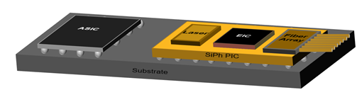
This is the promise behind CPO. This approach integrates optical transceivers directly on the same package as the switching ASIC, enabling ultra-short electrical traces and dramatically improving energy efficiency. A closely related approach, near-packaged optics (NPO) places the optics just off-package, but still much closer than conventional pluggable modules. Each approach has trade-offs, but both are being actively explored to meet the relentless demand for higher data rates.
While CPO presents a compelling solution to the growing data rate demands, it also introduces a new set of engineering challenges that must be addressed for practical deployment.
Key among these challenges is electronic-photonic co-simulation, essential to ensuring signal integrity across both domains; thermal management, as densely packed optical engines and ASICs generate significant heat; and long-term reliability, which becomes increasingly critical in data center environments that demand uninterrupted performance.
Moreover, realizing CPO will rely on advanced packaging technologies such as 2.5D and 3D-ICs. These platforms offer the physical integration capabilities required for such hybrid systems. Still, they bring design complexities — signal routing, thermal dissipation, mechanical stress, and yield — all of which now become integral to the success of CPO systems.
To address these challenges, simulation plays a crucial role in designing and validating CPO systems. Through end-to-end electro-optical co-simulation, engineers can gain insights into both time-domain behavior and frequency-domain performance, helping to evaluate signal integrity and overall system performance within the package.
In parallel, thermal simulation using 3D computational fluid dynamics (CFD) enables prediction of heat distribution and cooling efficiency, which is vital for managing the dense thermal loads in co-packaged architectures. Moreover, since reliability is closely linked to thermal and structural stress factors, simulation tools can assess material deformation, interconnect fatigue, and long-term component stability under operating conditions.
To support this complex, multidisciplinary design process, comprehensive multiphysics simulation tools and solutions enable verification, optimisation, and integration across the electrical, thermal, photonic, and structural domains.
- Powerful capabilities enable integrity analysis, especially in the optical and high-speed domains, helping to ensure seamless data transmission through photonic interconnects.
- For thermal and reliability management, advanced 3D thermal modelling tools enable detailed analysis. Additional solutions assist in analyzing thermal-induced stress and reliability risks at the chip and package level.
- Optical–thermal integration allows true multiphysics co-simulation, bridging optical and thermal effects for a more accurate prediction of real-world behavior.
- Optical design and simulation tools support the modeling and analysis of photonic integrated circuits (PICs) and optical I/O, enabling detailed design exploration of optical paths and interconnects.
- Finally, circuit-level and system-level platforms facilitate the co-design of electronic and photonic integrated circuits, enabling system-level simulation and chip-to-chip coupling for complete end-to-end performance evaluation.
These tools empower engineers to confidently design, optimise, and validate co-packaged optics architectures, ensuring that performance, reliability, and thermal constraints are addressed early in the design cycle.